


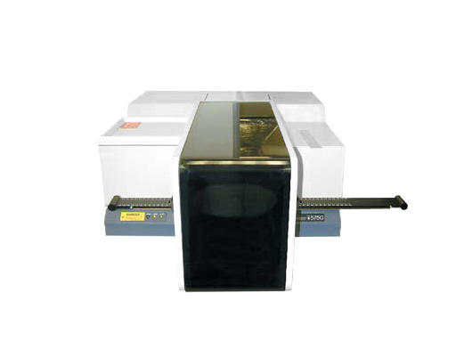
Nanometrics presents the QS-1200 desktop system for dopant monitoring, epi thickness measurement. and other applications.
The QS-1200 is designed for advanced semiconductor fabs performing material characterization in silicon growing and device manufacturing areas. It provides a new level of integration of the FTIR technique utilizing proven optical technology, and a manual wafer tray to accommodate SEMI standard wafer sizes of 100, 125, 150, 200, and 300 mm. Odd shaped wafer pieces,and 2 mm thick silicon slices can also be used on the QS-1200. An Elvailable option is a single wafer mapping (r, theta) stage for all the above wafer sizes.
Please contact our sales for detail information
+86-21-64813366
sales@quatek.com.hk


