


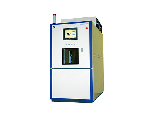
Specifically for compound semiconductor (GaN & GaAs) Automated mass production of plasma assisted chemical vapor deposition systems with small footprint, high throughput and low maintenance costs. More than 40 years experience in equipment manufacturing experience
State of Art Design for Large Quantity Production & COO Reduction
VDS-5800SNC-L has the capability to accommodate 40% larger batch capacity as compared to VDS-5800SNC through maintaining deposit quality and uniformity to be identical.
Superior film thickness and film quality uniformity
Gas-Cleaning after every Batch processing contributes to high quality and film thickness uniformity improvement.
Superior film thickness and film quality repeatability
The below figure is a graphic of the repeatability of 200batches.(Deposition→Cleaning→Deposition)
refractive index and film thickness is very good repeatability.


Stress Control
The below figure is a graphic of the changes of stress.
Stress is controlable by RFfrequency control.

VDS-5800SNC | VDS-5800SNC-L | ||
Wafer Charge | 2inch | 30 | 42 |
3inch | 15 | 21 | |
4inch | 9 | 12 | |
6inch | 5 | 8 | |
Suscepter | Φ527mm | Φ670mm | |
Frequency | 400kHz/13.56MHz | ||
Deposition Rate Range | 5~110nm/min | ||
Film Stress Control | Yes | ||
Uniformity | 3%以下 | ||
Up Time | 97%以上 | ||
Option | RealTime Process Monitor | ||


