Micro-spot size Reflection and Transmission Spectrophotometry
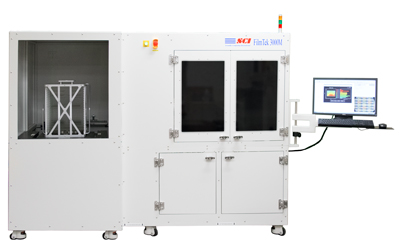
The FilmTek™ 3000M combined reflection-transmission metrology system was developed for efficient and accurate measurement of patterned films deposited on transparent substrates. The FilmTek™ 3000M utilizes allows for a small spot size down to 2 µm, and can be equipped with a large custom stage for flat panel display applications.
Conventional optical metrology systems which utilize a high power objective for sub-15µm spot measurements are prone to significant signal degradation and optical artifacts, limiting their use for patterned samples, non-uniform films, and thick films. The patented optical design of FilmTek™ 3000M maintains high signal fidelity even during small spot measurements by allowing for a sub-10µm spot with a low power objective. Avoiding the use of a high power objective is critical for limiting the angular spectrum of the collected light and maximizing the coherence of both spectral reflection and transmission.
FilmTek™ 3000M capabilities can be expanded to perform fully-automated imaging-based critical dimension (CD) measurement of patterned samples. This option allows for simultaneous CD and film thickness measurement.
FilmTek™ 3000M is a fully-integrated package, with advanced material modeling software to make even the most rigorous of measurement tasks reliable and intuitive.
Key Features:
- Spectroscopic reflection
- Spectroscopic transmission
- 5nm to 350µm film thickness range
- 2µm spot size (5×10µm standard)
- Automated stage with autofocus
- Camera for imaging measurement location
- Pattern recognition
Measurement Capabilities:
FilmTek™ 3000M incorporates SCI’s generalized material model with advanced global optimization algorithms for simultaneous determination of:
- Multiple layer thicknesses
- Indices of refraction [ n(λ) ]
- Extinction (absorption) coefficients [ k(λ) ]
- Energy band gap [ Eg ]
- Critical dimension (CD) measurement
Optional Features:
- Automated flat panel/wafer handling
- Flat panel total thickness variation (TTV) measurement
- SECS/GEM