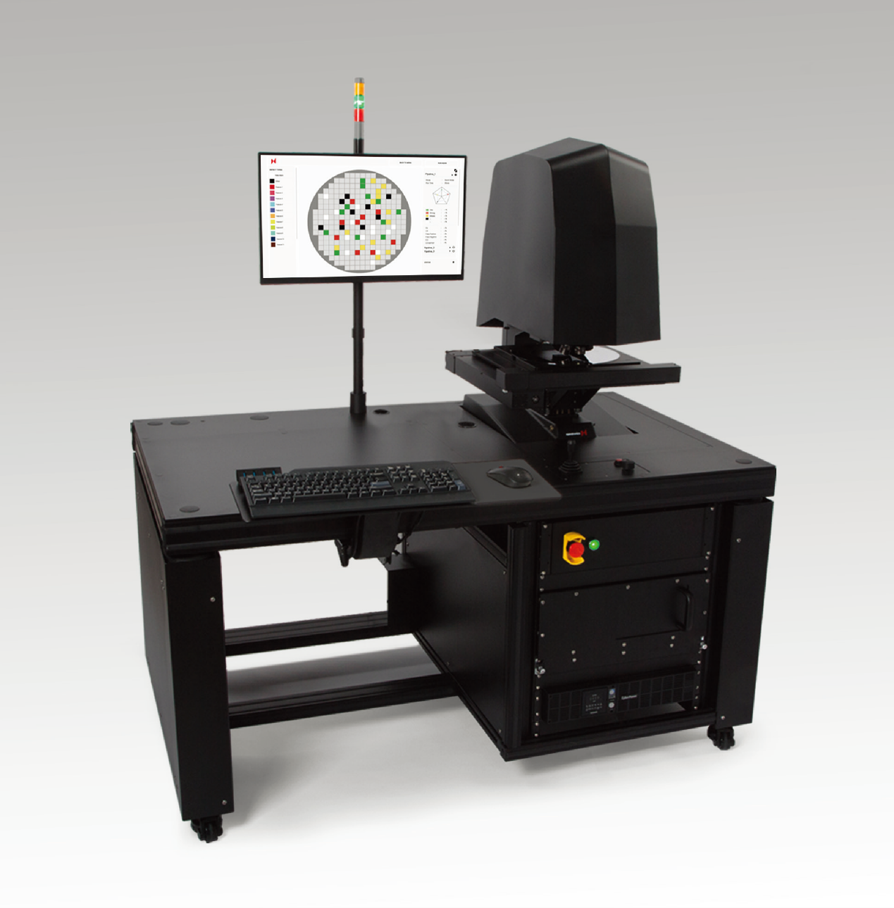


These are many examples of how the use of Nanotronics tools are actually transforming the way companies operate factories. These are four short examples.
Customer Use Case 1
One of the largest suppliers of silicon carbide wafers for compound semiconductors purchased one of the very first nSpec® tools and has since purchased 2 more. The customer has been using an automated scanning optical microscope and custom software for analyzing crystalline defects on the substrate. In order to detect and classify defects, a destructive test was needed. The customer would chemically etch the wafer in order to enhance the contrast between the defects and the background substrate. Being a destructive test, only a small number of wafers, each with costs of several thousand dollars, could be inspected. This compromised quality and provided no active way of doing process control, leading to disputes along the supply chain as causality and responsibility were always being questioned.
nSpec® was able to address this problem by using focus, lighting, movement, and classification algorithms to analyze an un-etched wafer. These solutions allowed for the first process control tool for defect detection at this facility. This is an application that can be applied to all compound semiconductor customers including all LED manufacturers who currently do not have a method for non-destructive testing.
Customer Use Case 2
The flexibility of the nSpec® hardware platform along with its ability to train a neural net allow for the customer to no longer be reliant on feature and defect libraries. A good example of this is when one of the world’s largest companies added the capability of photoluminescence to nSpec® by providing a ring of lasers to the frame of the tool. With this they were able to combine two completely different areas of the fab which were defect detection and classification with photoluminescence. This is one example of increasing throughput and ultimately yields by reducing time to move wafers as well as being able to address causality of faulty parts.
Customer Use Case 3
Randomly dispersed nanoparticles present many challenges as disagglomeration, distribution, and elimination of artifacts from the primary matrix often make scalability expensive or even prohibitive. A supplier to a pharmaceutical company that makes a cancer delivery system was using silica as an ingredient in the compound. The release mechanism involved the attraction of a cancer cell to the active ingredient. When the silica created agglomerates over 1 micron, the target was misdirected. Using nSpec®3D the customer is now able to measure and adjust the mix cycle when creating the compound. This trial was recently completed, and the first nSpec®3D just purchased by this customer. This could lead to hundreds of nSpec®3D sales with little or no additional customization of the tool.

Customer Use Case 4
The ability to combine testing of many layers in a customer process, in a single testing bay, with an engineer overseeing, is an important step in the evolution of many semiconductor fabs. With one large customer we were able to physically reduce the footprint of the fab itself allowing for internal consolidation of resources by providing rapid die yield analysis on many layers of a 235 layer process. The client has recently acquired two other large semiconductor companies, and Nanotronics’ early successes with the client could result in hundreds of nSpec® orders as well as provide a model for the future of wafer production.

