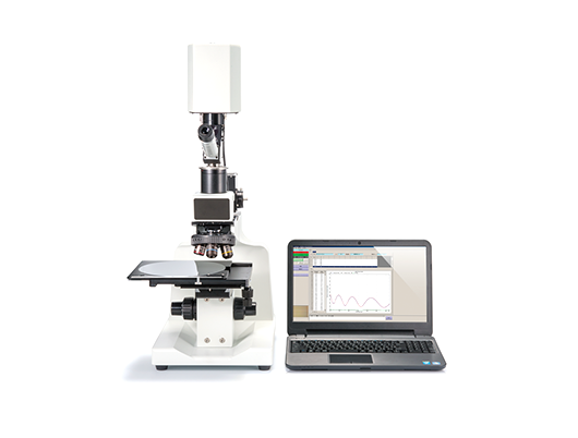


The TohoSpec 3100 is a state of the art, small spot spectroscopic reflectometer, built on a simple-to-use tabletop platform. A reliable solid state linear diode array is used to ensure measurement speed and accuracy. Incorporating core technology acquired from market leader Nanometrics, this system is specifically designed for a wide variety of R&D applications. The TohoSpec 3100’s Windows software interface is easy to use, and is supplied with a suite of measurement programs that handle most semiconductor films. The flexible software design makes it simple for the engineer to customize measurement programs and recipe jobs for more advanced applications. The TohoSpec 3100 delivers the same trusted results as its predecessors while offering the user enhanced versatility and data management.
Standard Features
Comprehensive Measurements
The 3100 provides scanning from 380nm to 800nm and can measure single layer films such as oxide, nitride, and photoresist, as well as multiple layer film stacks of up to three layers simultaneously. Measurements can also be made on a wide variety of other substrates including silicon, aluminum and gallium arsenide.
Dynamic Software
The 3100 software platform allows for the creation of unique single and multiple layer programs for proprietary films and film stacks utilized in modern semiconductor processes. With the ability to select film constants, scan ranges, and substrate types, the 3100 is the ideal tool for rapid measurement program development. Data management features, statistical analysis, histograms, and the ability to import and export data files are all standard.
Enhanced by W.Theiss SCOUT
Powerful and flexible SCOUT software provides increased measurement capabilities including: Simultaneous measurement of optical constant (n, k)
Simple and advanced dispersion models for optical material characterization:
• Cauchy: Transparent film (SiO2, SiN, PI, Photo Resist etc.)
• OJL model, Tauc-Lorentz: Interband transition models with ‘built-in’ Kramers-Kronig relation
• Extended Drude model: Conductive film, ITO, TiN etc
Optical models for film condition assessment:
• EMA: Surface roughness and Interface roughness etc.
• Graded: Nonhomogeneous in the direction of depth. Enhancement of the optical model for film condition.
Performance
Film Stack / Number of Films:Up to 3 layers simultaneously
Wavelength Range:380 - 800 nm (Standard)
380 - 850 nm (Thick film)
Film Thickness Range
Standard Configuration (5x):100 Å - 30 µm
Thick Film Configuration (5x):100 Å - 70 µm
Repeatability:2 Å
Film Type / n & k values:Obtained
Measurement Time:0.1 to 2.5 seconds/site (3100)
0.01 to 2.5 second / site (3100 T)
Data Management:Statistical data analysis,
Data export (ASCII)
Hardware Configuration
Wafer Sizes:Stage handles 3, 4, 5, 6, 8 inch wafers
Head Unit:Reflectometer Linear Array
Optics / Spot Sizes
5x (standard):50 µm (15 µm for Thick film)
10x (optional):25 µm (7.5 µm for Thick film)
50x (optional):5 µm (1.5 µm for Thick film)
100x (optional for Thick film):(0.75 µm for Thick film)
Optical Filters
Yellow cutoff filter:480 nm (measured at 50% light transmission)
Orange cutoff filter:560 nm (measured at 50% light transmission)