


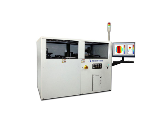
The MicroSense UltraMap UMS-300-BP is a semi- automated Wafer Measurement System which measures the thickness and TTV of wafers and substrates of any material, resistivity, thickness and surface condition with excellent repeatability. Wafers, up to 300 mm, are manually loaded into the measurement system; all wafer positioning and non-contact wafer measurements are fully automatic. The system handles either wafers only, or is configurable for handling wafers on tape in frame.
Applications
Measure Thickness of Thinned Wafers after backgrind – a vacuum wafer holder is used for measuring thickness of thinned wafers down to 100 microns, or thinned wafers on tape down to 50 microns.
Measure Thickness and TTV of Wafers On Tape – flexible software algorithm provides a method for determining wafer thickness and TTV even when wafer is mounted to tape or die attach film.
MicroSense UltraMap - A Better Approach to Wafer Measurement
Wide thickness measurement range – 50 μm to 3mm wafer thickness
Production friendly design – no cleanroom required - measure wafers at all steps during wafer making process
Integrated standards for in system auto-calibration
Air Bearing X-Y Wafer Stage for reliable, repeatable measurements
Measurement Technology
The UMS-300-BP uses two patented backpressure sensing probes for precise measurement of all materials conductive or non-conductive. The advantages of this sensing probe technology include:
Integrated, in system auto-calibration of backpressure sensors - no need for master wafers, no lost productivity for calibration
No need to adjust for different materials
Automatic adjustment to material thickness
| Measurement Parameters | Accuracy | Repeatability One Sigma | Display Resolution |
| Thickness: Flat Wafers (<100um Bow) Thickness: Center, Minimum, Maximum, Average | 0.5 μm | ± 0.015 μm | 0.1um |
| Wafer Specifications | System Configuration |
| Wafer Size: Any, including, and Custom and Saw-frame mounted. Wafer Thickness Range: 100μm - 3000μm Surfaces: Wafers - As Sawn, Lapped, Polished | Wafer Handling: Manual Wafer Measurement Location Positioning: Manual Calibration: Automated Wafer Measurement: Automated Reliability (MTBF): 50,000 Samples |
| Facilities Requirements |
| Dimensions: 18” width, 16” depth, 20” height. Separate PC, Monitor, Keyboard, and Mouse Weight: 100lbs Voltage: 110V for US, 200 – 250V options available. Single phase grounded polarized outlet required. Frequency: 50/60 Hz Current: 2A nominal, 10A peak Circuit Breaker: 10A UL489A certified breaker Air supply: Clean dry air or Nitrogen 40 – 60 PSI Fittings: ¼” compression fitting |


