


Automatic, non-contact measurement of filmed, patterned and bare wafers -150mm & 200mm diameter.
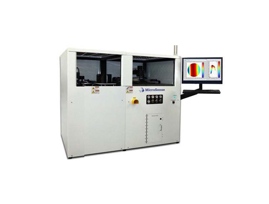
The MicroSense UltraMap UMA-C200-STR measurement system provides full wafer, high speed geometry measurement of silicon wafers using non-contact capacitance sensors with nanometer level thickness resolution. Over 120,000 data are measured on each wafer to generate high resolution wafer maps.
The system measures the thickness, flatness, bow and warp of the wafer in compliance with SEMI standards. MicroSense UltraMap StressMap software provides accurate measurement of wafer stress based on high resolution wafer pre- and post deposition shape data.
The system automatically calibrates before and after each wafer is measured for best repeatability. Wafers are robotically loaded into the system, then automatically positioned during measurement by a precision direct drive air bearing X-Y stage.
UltraMap Measurement Software – a powerful, versatile wafer data analysis tool for precise process control
MicroSense UltraMap software provides a complete range of SEMI standard wafer thickness/flatness/shape measurements, including local and global flatness, and wafer stress. Both 2D and 3D wafers maps are provided. MicroSense Stress Map software provides a comprehensive set of wafer stress metrics based on full wafer mapping.
Full Wafer Local Stress Mapping for Process Optimization
Stress measurement of the critical thin film layers is required for process tool monitoring, optimization and matching for yield maximization.
Stress non-uniformity can have an effect on device performance.
Stress non-uniformity can lead to device failure due to peeling/cracking.
High stress causes chucking problems (defocus) at lithography because of excessive wafer bow.
As manufacturers transition from 150mm silicon wafers, stress metrology for 200mm wafers helps to reduce wafer edge exclusion zones to increase yield, it is a useful tool for solving yield issues with near edge die.
The MicroSense UltraMap UMA-C200-STR provides comprehensive data for every wafer measured:
Wafer thickness
Average wafer bow and warp, Average wafer radius of curvature
Average wafer film stress
2D Local Stress Map with Min and Max values
3D Local Stress Map with Min and Max values
Local Line Stress Profiles with specified orientation, including Min and Max values.
All data and maps are exportable
| Measurement Parameters | Accuracy | Repeatability One Sigma | Display Resolution |
| Thickness: Center, Minimum, Maximum, Average | ± 0.10 μm | 0.05 μm | 10 nm |
| Global Flatness: | ± 0.05 μm | 0.05 μm | 10 nm |
| TTV | |||
| TIR | |||
| FPD | |||
| Local Flatness: | ± 0.05 μm | 0.05 μm | 10 nm |
| Local Thickness Variation (LTV) | |||
| Local Total Indicator Reading (LTIR) | |||
| Local Focal Plane Deviation (LFPD) | |||
| Bow and Warp | 0.25 μm + 0.5% of reading | 10 nm | |
| Bow | |||
| Warp | |||
| Sori |
Measurement Throughput (Wph) – full wafer mapping
150mm/65 200MM/50
Data Analysis
Measurement Parameters: Thickness, TTV, TIR, LTV, Bow, Warp
Wafer Maps: Contour, 3D Surface, Site LTV, Wafer Stress
| Wafer Specifications | System Configuration |
| Diameters: 150mm, 200mm Diameter Tolerance: ± 0.5mm Thickness Range: 300 to 1400 um Dynamic Range: Thickness: ± 150 um Bow/Warp: ± 250 um Surfaces: Sawn, Lapped, Polished Fiducials: Semi Flat, Notch | Wafer Handling: Robotic Measurement Positioning: Precision Air Bearing Pre-aligner: Included OCR Reader: Optional SECS/GEM: Optional Cassette Stations: 2 cassettes standard Calibration: Automated Reliability (MTBF): 10,000 |