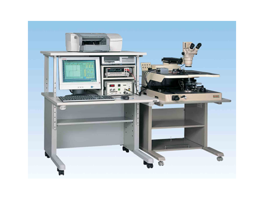


Model 400S allows zapping HBM or MM ESD stress to various shape DUT, then automatically detect damage or degradation by very little programming. Even designer simply tests the ESD performance of a new design any time.
ESD Performance Test from Wafer to package
Process Monitoring by periodical wafer test
Allows correlation test between die location and ESD performance
Multiple return allows ESD current path verification
Enables rapid ESD performance test of new devices
Decreases device development time
1. Source Measure unit/Damage criteria
Polarity : Positive, Negative
Force Voltage
Range : 0 to 30V
Digits : 3
Minimum Step : 10mV
Tables: 4 tables (Vf-A to Vf-D)
Current measurement
Range : 0 to 200mA
Digits : 3
Resolution : 10nA (*)
Averaging : 1, 2, 4, 8, 16, 32 times
Start Range : 1, 10, 100, 1000μA
Limiters : 2, 20, 200mA
Sample points : 1 to 91 samples
Measurement speed : Fast/slow
Damage detection points : 1 to 10 points
Damage criteria : Initial current * (1 to 100)%
+ (100nA to 1mA)
2. ESD pulse
Polarity : Positive and Negative
Period : About 1 sec
Repetition : 1 to 100 times
Charge Removal : Supported
Zap voltage
HBM: 0 to 400V/5Vstep
400 to 4000V/50V step
MM: 0 to 400V/5V step
400 to 4000V/50V step
Accuracy : 1% of setting±5V
Waveform: MIL, JEDEC, JEITA, others
3. Test Program
Semi-auto test
Automatic test
V/I curve measurement
ESD zapping