This article is reproduced by Ren Gang and Wang Fei from the wechat official account VertexVentures.
On April 20, the National Development and Reform Commission (NDRC) officially announced the scope of "new infrastructure" for the first time, officially setting the development direction of seven areas including 5G infrastructure, artificial intelligence and industrial Internet. Driven by the construction demand, a large number of technological innovation enterprises will also usher in the window period of development.
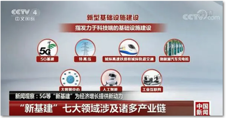
As an emerging industry, "new infrastructure" is connected with the constantly upgrading consumer market at one end and the rapid development of technological innovation at the other. It is worth noting that, whether 5G, new energy vehicles or industrial Internet, the construction of various industries of "new infrastructure" are closely related to the development of semiconductor technology. Such as:
The rf semiconductor with gallium nitride (GaN) as the core supports the construction of 5G base station and industrial Internet system.
Power semiconductors with silicon carbide (SiC) and IGBT as the core support the construction of new energy vehicles, charging piles, base station/data center power supply, uHV and rail transit systems.
The SOC chip with AI chip as the core supports the construction of data center and artificial intelligence system.
It is not hard to see that gallium nitride (GaN) and silicon carbide (SiC) led by the third generation semiconductor is the core material to support the "new infrastructure". With the support of "new infrastructure" and domestic substitution, domestic semiconductor manufacturers will usher in great development opportunities.
As an observer of China's semiconductor industry, Xiangfeng Investment brings a "Third Generation Semiconductor Industry Research Report" this time, which will discuss the following issues, divided into two phases:
A, the third generation of semiconductors compared with the first generation, the second generation of progress?
Why gallium nitride (GaN) and silicon carbide (SiC) are popular in the third generation of semiconductors?
What are the application scenarios of gallium nitride (GaN) and silicon carbide? How big is the market? What are the factors driving both growth?
Second, what are the key technologies of the third generation semiconductor chip in each link of the industrial chain (substrate, epitaxial, design, manufacturing, packaging)?
What are the major third generation semiconductor manufacturers at home and abroad?
This is the first part of the report.
Research on the third generation semiconductor industry
- the last -
The author | Ren Gang, wang
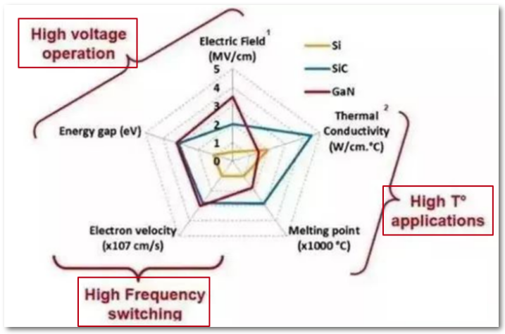
1. the third generation semiconductor in the breakdown electric field, thermal conductivity, electron saturation rate and radiation resistance ability of comprehensive improvement
The use of semiconductors dates back to the 1950s and 1960s and has gone through three iterations (see chart).
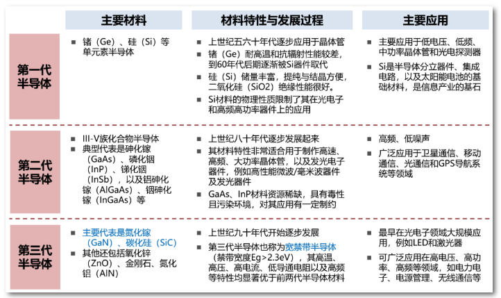
Compared with the first generation and second generation of semiconductor materials, the third generation semiconductor material have wider band gap width and higher breakdown electric field, higher thermal conductivity, higher electron saturation rate and higher ability to resist radiation, more suitable for making high temperature, high frequency, high power and resistance to radiation devices, can be widely used in high voltage, high frequency, high temperature and high reliability etc, Including radio frequency communication, radar, satellite, power management, automotive electronics, industrial power electronics, etc.
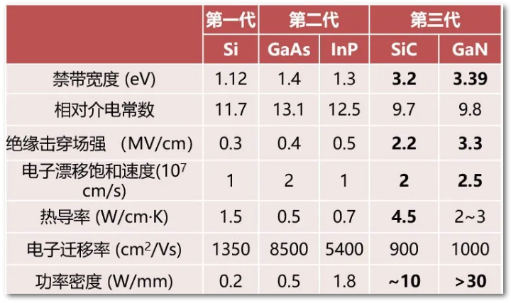
Comparison of main performance parameters of three generations of semiconductor materials
2. Gallium nitride (GaN) and silicon carbide (SiC) are the main choices for large-scale commercial use at present
Among the third generation of semiconductor materials, silicon carbide (SiC) and gallium nitride (GaN) are the most mature materials, which are the main choices for large-scale commercial use at present.
It can be clearly seen from the commonly used Figure of Merit (FOM) in the following table that SiC and GaN have greatly improved their functions and characteristics compared with the previous two generations of semiconductor materials.
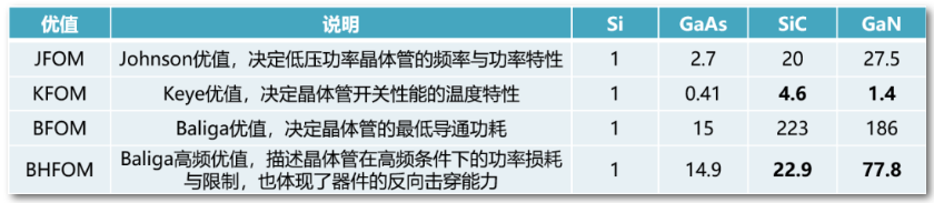
* The above optimal values are normalized with Si material as unit 1
GaN and SiC have their own advantages and disadvantages in material properties, so they have different emphasis and complement each other in application fields.
The high frequency Baliga value of GaN is significantly higher than that of SiC, so GaN has advantages in the field of high frequency small power, concentrated below 1000V, such as communication base station, millimeter wave, etc
The Keye value of SiC is significantly higher than that of GaN, so SiC has advantages in high temperature and large power fields above 1200V, including electric power, high-speed rail, electric vehicles, industrial motors and so on
GaN and SiC can be used to compete with traditional Si based devices in low and medium power fields
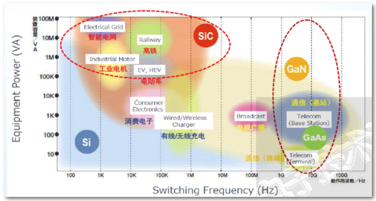
GaN and SiC application fields
3. Application scenarios, market size and growth drivers of gallium nitride (GaN)
GaN devices mainly include radio frequency devices, power electronic power devices, and photoelectric devices. The commercial application of GaN began with LED lighting and lasers, which are more based on the direct band gap characteristics and spectral characteristics of GaN. Related industries have been developed very mature. Rf devices and power devices are the main applications of GaN wide band gap semiconductor.
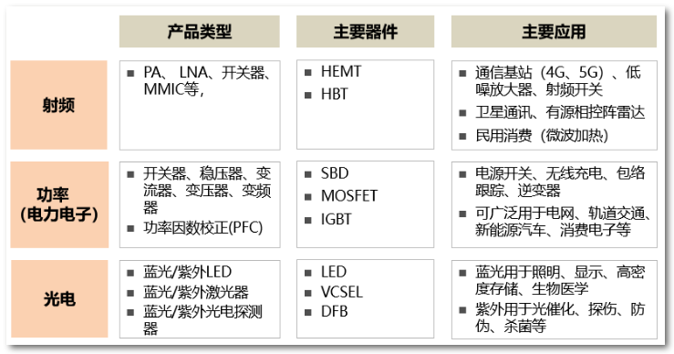
GaN rf device
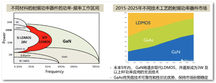
The main technologies of RF devices include silicon based RF CMOS, Si-LDMOS, GaAs and GaN schemes.
· Silicon-based RF CMOS is suitable for low frequency and low power fields. In Bluetooth, Zigbee applications dominate, some WiFi and low-end phones also use this solution
· GaAs solutions are suitable for low-power applications, usually below 50W, and are currently one of the main technologies for RF chips in 4G/LTE base stations. Most mobile phones also use GaAs for their power amplifier chips. In the short term, 5G mobile terminals are still GaAs solutions
· Si-ldmos (Lateral diffusion MOS) is one of the main rf chips for 4G/LTE base stations. The disadvantage of LDMOS device is that there is a limit of working frequency, the highest effective frequency is below 3.5ghz
· GaN scheme makes up for the defects of GaAs and SI-LDMOS, and has obvious advantages in the high power and high frequency rf market, especially in the range of high frequency (greater than 8 GHz) and medium power (10W~100W)
Data source: Yole
Application advantages of GaN RF devices:
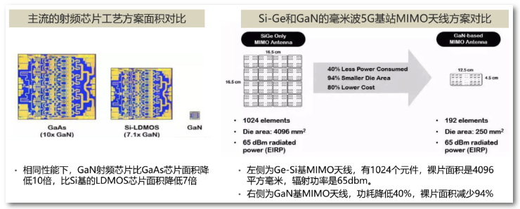
· GaN's advantage in power density makes the chip size greatly reduced
· 5G base station will use multiple multi-receiver antenna array scheme, GaN rf devices have a huge improvement on the power consumption and size of the entire antenna system
· In high power, high frequency rf applications, higher bandwidth, faster transmission rate, and lower system power consumption
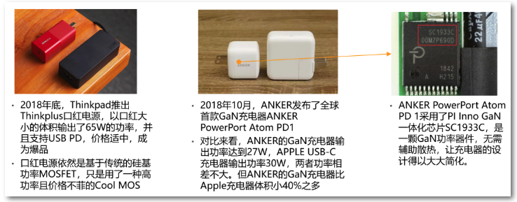
In addition, GaN rf power transistors can be used as a new solid-state microwave source to replace the traditional 2.45ghz magnetron in consumer electronics and industrial applications from microwave ovens to high-power welders.
Source: Qorvo
Market size of GaN RF devices:
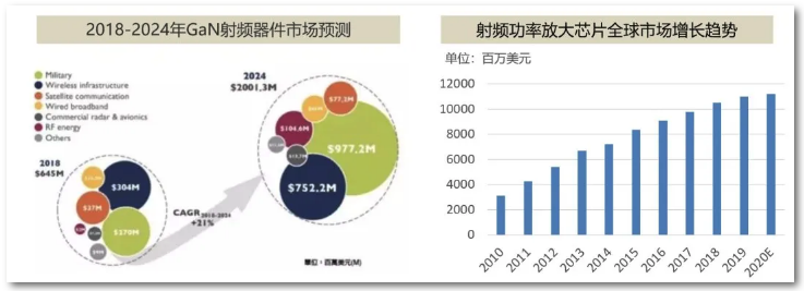
"The global market for GaN RF devices is expected to grow to $2 billion by 2024, although its share in the overall $10 billion RF chip market is still small, but the growth is expected."
According to Yole's forecast, the GaN RF device market is expected to grow to $2 billion by 2024 with a 6 year CAGR of 21%. The main market growth is in wireless communications infrastructure and military. The spread of 5G will push the WIRELESS communications market for GaN to $750 million
It should be pointed out that the market size of the entire semiconductor RF devices is in the tens of billions of dollars. GaAs devices still occupy the majority of the market share. In 2014, the global rf power amplifier chip (PA) market size was $7.39 billion. Due to the obvious performance advantages of GaAs PA over Si based CMOS PA, gallium Arsenide PA output value market accounted for 94%. The total PA market is expected to grow to $11.416 billion in 2020, with a cagR of 7.51% from 2014 to 2020, benefiting from mobile terminal upgrades and the continued development of the Iot industry
Data source: Yole, IBS
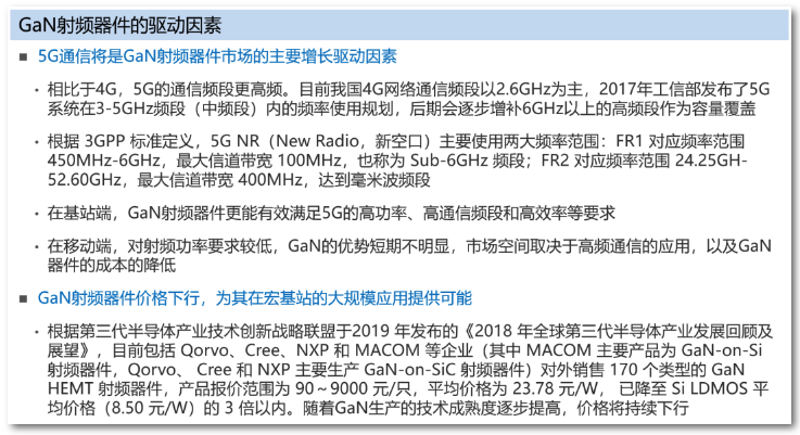
Driving factors of GaN RF devices:
On the demand side, 5G communications will be the main growth driver for the GaN RF device market.
On the supply side, GaN on SiC, GaN on Si technology continues to mature, so that GaN power devices have a higher cost performance, open the application space.
GaN power device
GaN power device is distinguished from the GaN rf power chip mentioned above. It mainly refers to work at high voltage and large current, and has little relation with high frequency and rf. The most common application of this type is power-related chips.
Power devices are mainly metal-oxide-semiconductor field effect transistors (MOSFET). Unlike other transistors that rely on current to drive, MOSFET is a voltage-driven device. As long as a suitable voltage is applied at the gate, MOSFET will turn on. This characteristic makes MOSFET in AC/DC switching power supply, variable speed motor, fluorescent lamp, DC/DC converter and other equipment has an irreplaceable role.
Main applications of GaN power devices:
· Consumer electronics: GaN due to high power density and good temperature characteristics, can be used in the power supply of small volume and high power output, in addition to better switching characteristics
· Data center power systems: Data centers contain many high-powered servers that typically require high current and low voltage, coupled with cooling systems that are expensive to use. The conversion of high voltage to lower direct current is often used for multiple DC-DC conversions, with efficiency decreasing at each stage of power conversion. If high voltage devices can be used for conversion, the frequency of voltage conversion can be reduced, so as to improve the conversion efficiency of the whole system
· Photovoltaic inverter: The use of GaN power devices, operating at a switching frequency of more than 100 kHz, can greatly improve the inverter efficiency of the system
· Other areas include DC-DC converters, POL converters, as well as motor drives and Class D high-power audio amplifiers
Market size of GaN power devices:
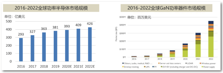
The global power semiconductor market was 32.7 billion US dollars in 2017 and is expected to reach 42.6 billion US dollars by 2022. Industrial, automotive, wireless and consumer electronics are the top four end markets.
GaN devices in the entire power semiconductor market is still very small. The market size of GaN power devices was approximately us $12 million in 2016 and is expected to grow to US $460 million by 2022, with a 79% CAGR. The growth will come from applications such as power management, new energy vehicles, LiDAR, wireless power and packet tracking.
As GaN on Si technology matures and costs decrease, the potential market space for GaN power devices will continue to expand. GaN is expected to replace Si MOSFET, IGBT and other silicon based power devices in low and medium power. According to Yole estimates, in the low voltage market of 0~900V, GaN has great application potential, which occupies about 68% of the whole power market, according to the overall market of $40 billion, the potential market of GaN power devices is more than $27 billion.
Data source: Yole, IBS
4. silicon carbide (SiC) application scenarios, market size and growth drivers
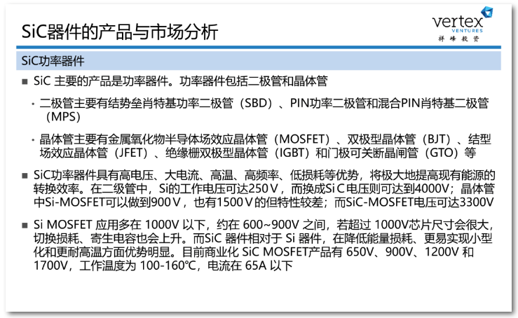
MOSFET and IGBT are the most widely used power devices. SiC began to be developed in the 1970s. 2001 SiC SBD commercial, 2010 SiC MOSFET commercial. SiC IGBT is still under development.
SiC can greatly reduce the switching loss in power conversion, so it has better energy conversion efficiency, easier to achieve module miniaturization, and more high temperature resistance.
Main applications of SiC power devices:
· Smart grid: the main applications of SiC power devices in smart grid include HVDC converter valves, flexible HVDC converter valves, flexible AC transmission devices, HVDC circuit breakers, power electronic transformers and other devices. At present, SiC devices have been applied in middle and low voltage distribution networks. In the future, flexible transmission and transformation with higher voltage, larger capacity and lower loss will have a great demand for SiC power devices above ten thousand volts
· Rail transit: mainly used for traction converters, power electronic voltagers, etc. Using SiC power devices can greatly improve the power density and work efficiency of these devices, which will contribute to significantly reduce the load system of rail transit
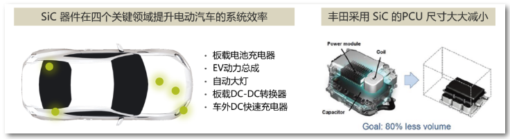
· New energy vehicles: SiC power devices have great advantages in the field of electric vehicles. The high temperature characteristics and high thermal conductivity of SiC power devices can significantly reduce the volume and cost of radiators. Their high frequency characteristics help improve the power density of motor drivers, reduce volume, reduce weight, and promote novel topology applications in motor drives, charging piles, and on-board chargers
· Photovoltaic, wind power: at present, the international photovoltaic grid-connected equipment market is the second largest application market of SiC power devices, accounting for more than 30% of the SiC power device market. SiC photovoltaic inverter efficiency can reach more than 99%, energy conversion loss can be reduced by 50%, which will greatly reduce the cost and volume of the inverter. Fan grid-connected equipment has a great demand for middle and high voltage SiC power devices, which can replace silicon devices in series or topological cascade, significantly reduce the volume of the device, and greatly improve the efficiency and reliability of fan converters. It is expected that by 2020, SiC power devices will enter the fan grid-connected equipment market
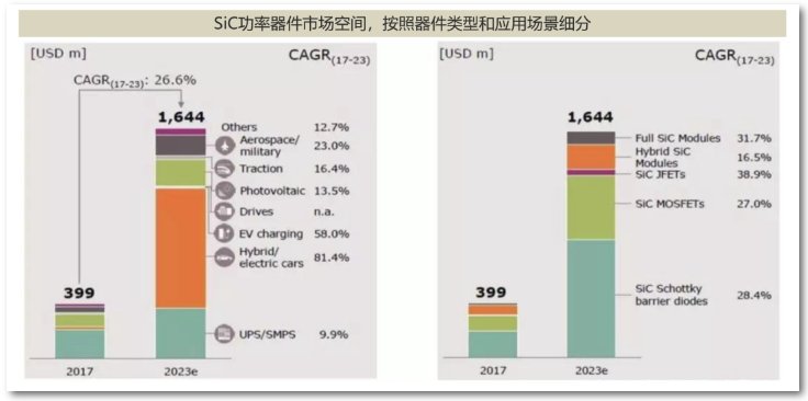
Market space of SiC power devices:
The global SiC power semiconductor market totaled $399 million in 2017. The total SiC power semiconductor market is expected to reach us $1.644 billion by 2023. From the product point of view, SiC SBD diode and SiC MOSFET will become the most widely used products. SBD diodes are widely used in various power supplies to achieve power factor correction (PFC) and other functions. The main use of SiC MOSFET is to replace Si IGBT in many application scenarios.
Data source: Infineon
Market space and driving factors for SiC power devices:
New energy vehicles are the main growth drivers of SiC power devices market. At present, the application of SiC devices in new energy vehicles is mainly power control unit (PCU), inverter, DC-DC converter, car charger and so on.
· PCU: This is the central nerve of the vehicle electric system, which manages the flow direction and transmission speed between the electric energy in the battery and the motor. Traditional PCUs are made of silicon. As for the use of SiC raw materials can significantly reduce power loss, about 10%, but also can greatly reduce the size and weight of the system
· Inverter: SiC can greatly reduce the size and weight of the inverter, lightweight and energy saving. At the same power, the package size of the all-sic module is significantly smaller than that of the Si module, and the switching loss can be reduced by 75%. In 2018, tesla Model3 inverter uses ST produced sic mosfets, each inverter includes 48 sic mosfets. The body of the Model3 is 20 percent smaller than the ModelS
· Car charger: SiC is accelerating penetration into car charger field. According to Yole statistics, as of 2018, there are more than 20 automakers in their own car chargers using SiCSBD or SiCMOSFET, this market is expected to maintain 44% growth before 2023
Data source: Cree official website; Geekcar
With the reduction and improvement of defects and quality of 6-inch SiC single crystal substrates and epitaxial wafers, SiC devices can be fabricated on the growth line of the existing 6-inch Si-based power devices, which further reduces the cost of SiC materials and devices and promotes the popularity of SiC devices and modules.
The next issue will explain the key technologies of the third generation semiconductor chip in each link of the industrial chain (substrate, epitaxial, design, manufacturing, packaging), as well as the industrial map at home and abroad.
This article is reproduced by Ren Gang and Wang Fei from the wechat official account VertexVentures.